Scanning Electron Microscope (SEM)

Brand / Model: Thermo Fisher Scientific / Apreo S
Description: Scanning Electron Microscopy (SEM) is an advanced analytical technique used to obtain high-resolution images of sample surfaces and to analyze their chemical composition. The Thermo Fisher Scientific Apreo S SEM available at our center is a high-performance system equipped with a field emission gun (FEG), providing 1 nm resolution at 1 kV. Its wide operating voltage range and advanced detector configuration enable detailed characterization of a broad variety of materials.
Working Principle: In SEM, electrons emitted from the source are focused by electromagnetic and electrostatic lenses within a vacuum column and directed onto the sample surface. The interaction between the electron beam and sample atoms generates secondary electrons, backscattered electrons, and characteristic X-rays.
-
Secondary electrons (SE) provide detailed information about surface topography.
-
Backscattered electrons (BSE) reveal compositional contrast based on atomic number differences and enable crystallographic analysis through EBSD.
-
The generated X-rays are collected by an EDS detector and used for Energy-Dispersive X-ray Spectroscopy (EDS) to perform elemental analysis.
Instrument Features
-
Electron source: Field Emission Gun (FEG)
-
Accelerating voltage: 0.2 – 30 kV
-
Resolution: 1 nm at 1 kV
-
Revolutionary compound final lens combining electrostatic and electromagnetic immersion
-
High contrast and signal selection at low voltage and beam current
-
Energy and charging filtering for insulating samples
-
Optional low vacuum mode up to 500 Pa chamber pressure
-
High performance on tilted, topographic, and beam-sensitive samples
-
High resolution without beam deceleration
Detectors and Analysis Systems:
-
Trinity Detection System (in-lens & in-column)
-
T1 low in-lens detector
-
T2 high in-lens detector
-
T3 in-column detector
-
Everhart–Thornley Secondary Electron Detector (ETD)
-
Retractable under-lens Backscattered Electron Detector (BSED)
-
Low Vacuum Detector (LVD)
-
Pathfinder X-ray Microanalysis System
-
Thermo Scientific UltraDry EDS Detector
-
Thermo Scientific Quasor II EBSD Detector
-
Nav-Cam+™ chamber-mounted camera
Application Areas
-
Nanoparticle and nanostructure research
-
Metals, alloys, and coatings
-
Composite and ceramic materials
-
Powders and catalysts
-
Polymers and insulating materials
-
Crystallographic analysis (EBSD)
-
Elemental analysis and mapping (EDS)
-
Academic and industrial R&D studies
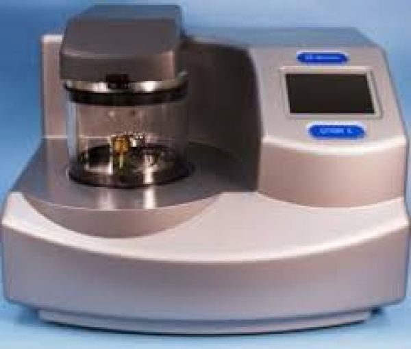
Magnetron Sputter Coating System – Quorum / Q150R S
The Quorum Q150R S magnetron sputter coating system is used for sample surface preparation prior to scanning electron microscopy (SEM) analysis. The system enables uniform thin film coating of sample surfaces with a gold–palladium (60%–40%) alloy under an argon atmosphere. Insulating or partially insulating samples are typically coated with a layer thickness of approximately 5–10 nm, which prevents surface charging and protects the sample from damage without obscuring fine structural details. Coating with high atomic number metals such as gold–palladium enhances image resolution in SEM imaging. However, such coatings are not suitable for EDS and EBSD analyses, as they may interfere with the detected signals and affect analytical results.
Device Specialist:
1. Lecturer Dr. Hasan Köseoğlu
E-mail: hasan.koseoglu@iste.edu.tr
Phone: 0 (326) 310 2843
2. Lecturer Mustafa Göktan Aydın
E-mail: goktan.aydin@iste.edu.tr
Phone: 0 (326) 310 2842